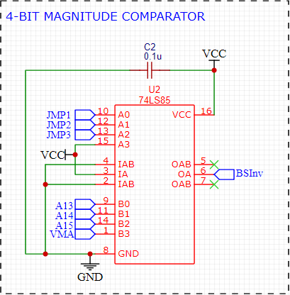
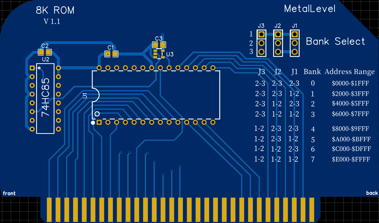
With a working cpu proto board, next up is the 8K rom card. Instead of designing a 4k, or 8k or 16K, or 32k board I decided to just create an 8k rom board, but have jumpers to map it into any of the 8 banks. This design uses three jumpers to bank select the decoded address for the board. I'm using a 74LS85 4-bit magnitude comparator to read the jumpers and match it to the A15,A14,A13 address lines. One other line, the VMA signal (Valid Memory Address) must also be a '1' before the rom is selected.

The output is BSInv, this is a '1' when
- JMP1 == A13 AND
- JMP2 == A14 AND
- JMP3 == A15 AND
- VMA == 1
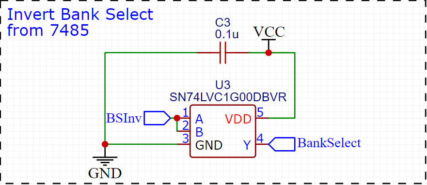
Because the rom chip is active low on the chip select, BSInv is inverted through a single gate 7400 AND chip.

Now we have a BankSelect signal which is the rom CS (chip select) pin.
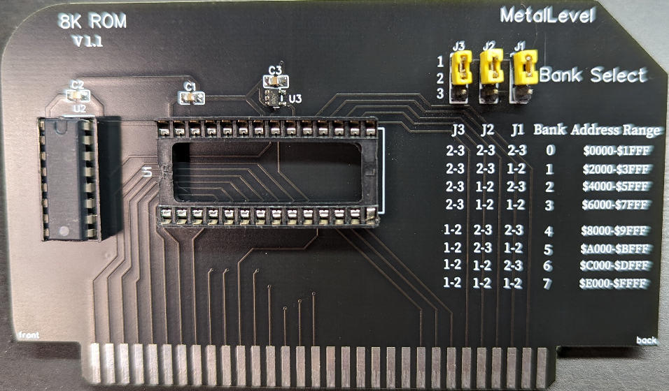
This is revision 1.1 of the board. Revision 1.0 didn't use VMA, which is definitely needed. I left off the part number for the rom on the silkscreen, I guess there will be a version 1.2 in the future. The rom I use is flash rom, 28c64. Any 27c64 eprom or 28c64 flash rom will work. I use the flash for a faster turn around with the eprom programmer.


This is jumpered for bank 7 address $e000..$ffff The MC6802 reset vector is the top 2 bytes of the address space ($FFFE, $FFFF) This is where at least one rom card must be.
Since you can select any bank for the rom card, you can have up to 8 installed, but realistically, only 7. Bank 0 is where the internal 128 bytes of ram of the CPU are mapped. It is still possible to put rom in bank zero, but the internal RAM would have to be disabled. Another advantage with bank selection is that the roms don't have to be contiguous.
--> ISA 8K RAM card
--> Previous
--> Home