I wanted to make some more pcbs so the next project was to make a pcb for the 8k rom and one for the 2k static ram.
I added pin headers to the top of the boards.
- A 2x8 pin header for the data bus.
- A 2x16 pin header for the address bus.
- A single pin header for the chip select and read/write signal.
The CPU signals are coming from the CPU board. The ROM card only needs the CS signal. The RAM card needs both CS and R/W
The address decoding was done external to these boards. The reason for the 2 rows of bus signals is so these boards could be daisy chained together.
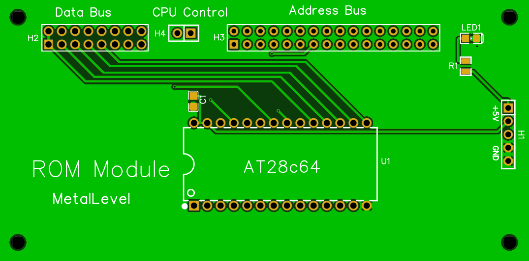
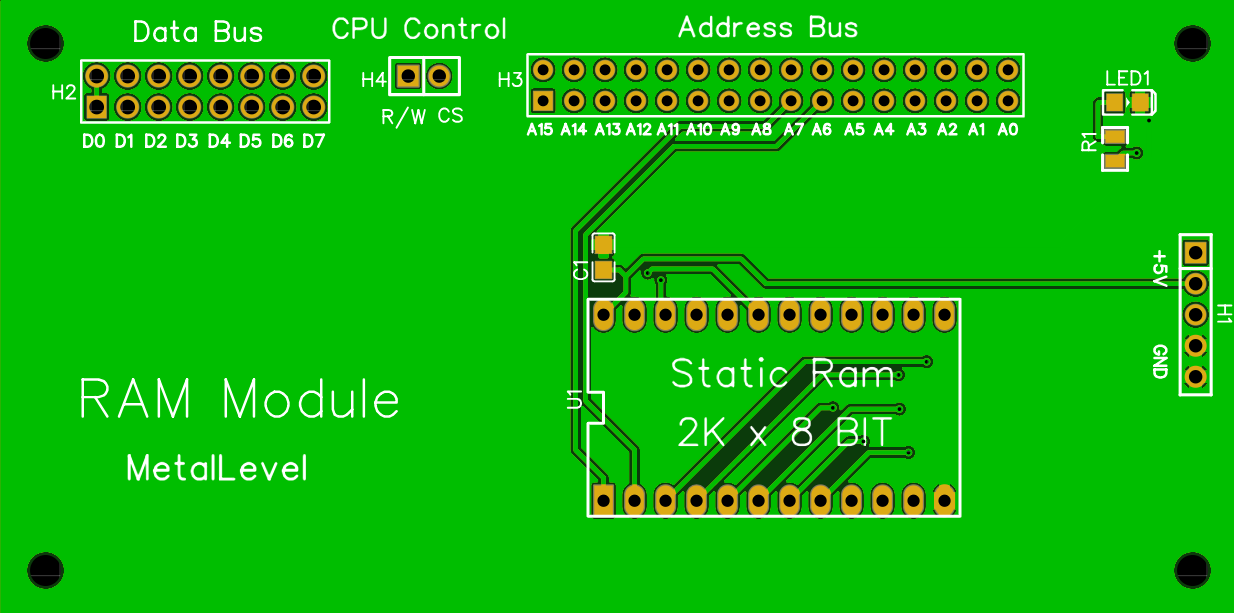
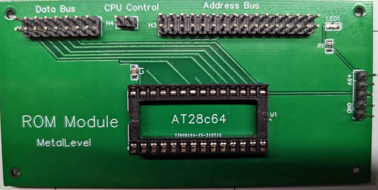
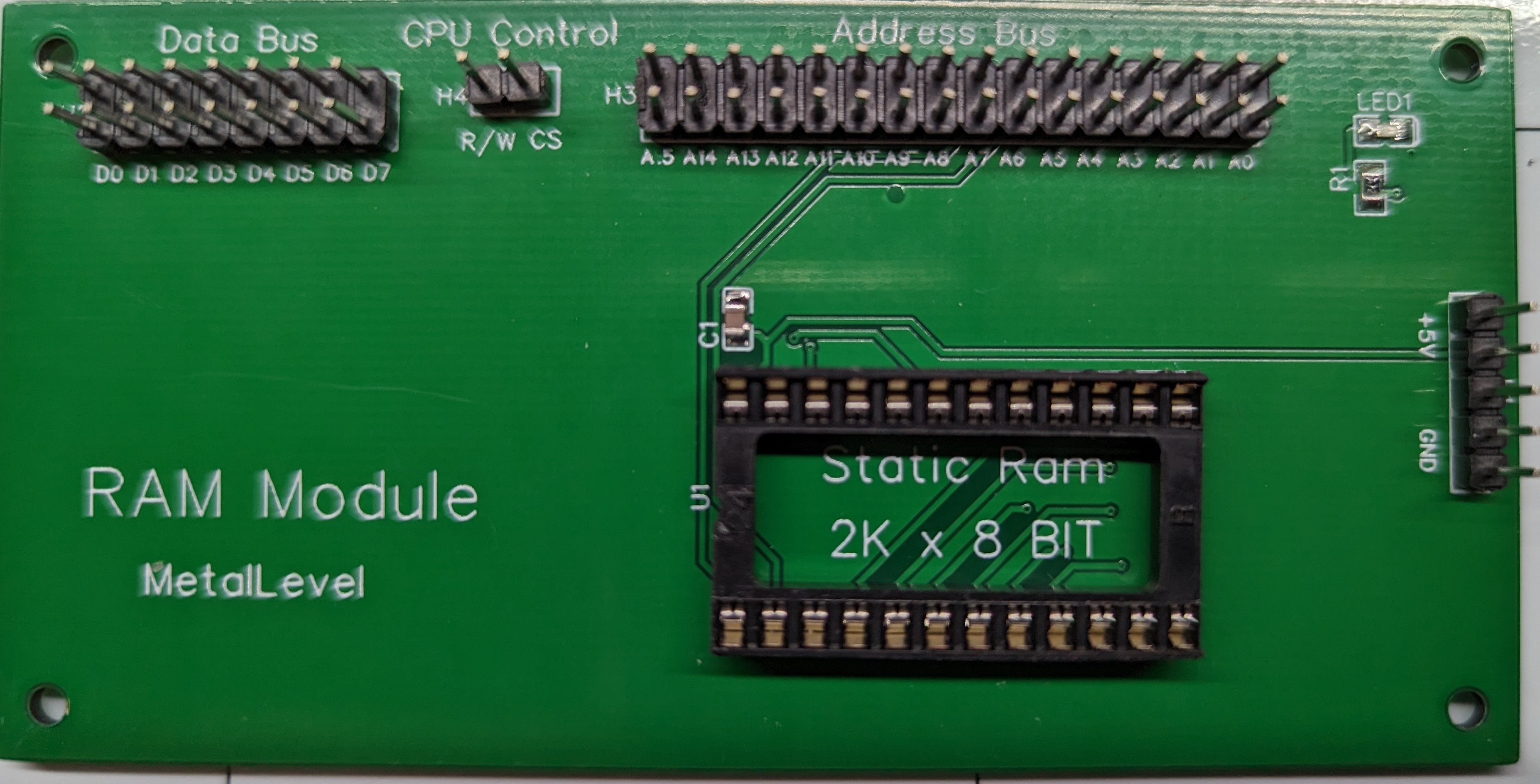
The ROM board was made first. As you can see I didn't put any labels on the silkscreen for the pin headers. With the RAM board I did label the pins.
The address decoding is done externally, currently by the cpu board, and hooked to the CS pin header. The idea here is to have these boards replace the current breadboard in the current design. Making them the same size with holes for standoffs, would allow a nice layout on the table.
I was still learning the pcb design software and these simple boards helped with that.
--> Previous
--> Home